
RF & Microwave PCB Manufacturer
As a specialized RF & Microwave PCB Manufacturer, PCBLion provides a true One-Stop Turnkey solution for high-frequency electronics. We combine advanced PCB fabrication (supporting Rogers/PTFE and hybrid stack-ups) with ultra-precise SMT assembly. Certified to IATF 16949 and ISO 13485, we deliver aerospace and automotive-grade reliability from prototype to mass production.
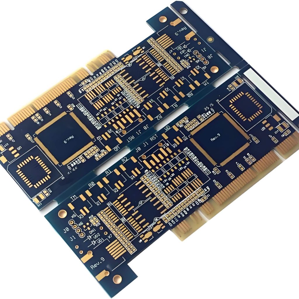
Why Choose Microwave PCB Boards?
Microwave PCBs provide excellent signal integrity and ultra-low insertion loss for high-frequency applications. They are the essential backbone for modern 5G, radar, and aerospace systems.
High-Frequency Performance
Optimized for signals from 1 GHz up to 110 GHz. Delivers minimal signal distortion, low insertion loss, and incredibly stable Dk/Df values for RF applications.
Advanced Thermal Management
Engineered with superior heat dissipation properties. Ideal for high-power RF amplifiers, supporting specialized cooling via copper coins and metal-backed structures.
Compact & Reliable
Allows for high-density component placement in smaller footprints. Highly resistant to extreme environmental factors, ensuring stable performance over decades of use.
PCBLion's RF & Microwave PCB Manufacturing Capabilities
| Items | Specification |
|---|---|
| Frequency Range | DC to 110 GHz (L, S, C, X, Ku, K, Ka, V, W bands) |
| Layer Count | 2-40 layers (Hybrid stack-ups available) |
| Materials | 70+ Resin Systems (Rogers, Taconic, PTFE, FR4) |
| Impedance Tolerance | ±3% to ±10% (Polar CITS500s tested) |
| Etching Tolerance | +/- 0.0005" (12.7µm) for un-plated 0.5oz copper |
| Registration Tolerance | +/- 0.001" (25.4µm) front-to-back core |
| Min Trace/Space | 0.075/0.075mm (3/3 mil) with LDI capability |
| Copper Weight | 0.5-2oz (18-70μm) |
| Board Thickness | 0.4-8.0mm |
| Max Panel Size | 600mm x 770mm |
| Surface Finish | Immersion Silver (Best for RF), ENIG, ENEPIG, ASIG |
Via Design for RF
| Parameter | Specification | Notes |
|---|---|---|
| Via Diameter | 0.3-0.5mm | Larger vias reduce inductance |
| Via Stub Length | <1mm for >10 GHz | Backdrilling required |
| Ground Via Spacing | <λ/10 around RF traces | Typically 1-2mm at 10 GHz |
| Via-in-Pad | Resin-filled and planarized | For BGA/QFN mounting |
Why Hybrid Stack-ups?
Pure Rogers boards can cost 3-5x more than FR4. A hybrid stack-up (Rogers outer layers + FR4 core) provides 80% of the performance at 40% of the cost.
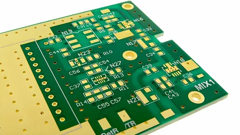
5G small cell antennas, Wi-Fi 6E routers, GPS modules
Layer 1: Signal (Rogers 4350B, 0.254mm)
Layer 2: Ground (Rogers 4350B)
---Core: FR4 (Shengyi S1000-2, 1.0mm)---
Layer 3: Power (FR4)
Layer 4: Signal (Rogers 4350B, 0.254mm)
Automotive radar modules, mmWave 5G base stations
Layer 1: RF Signal (Rogers 4003C, 0.203mm)
Layer 2: Ground (Rogers 4003C)
---Core: FR4 (Isola 370HR, 0.8mm)---
Layer 3: Power
Layer 4: Digital Signal
---Core: FR4---
Layer 5: Ground (Rogers 4003C)
Layer 6: RF Signal (Rogers 4003C, 0.203mm)
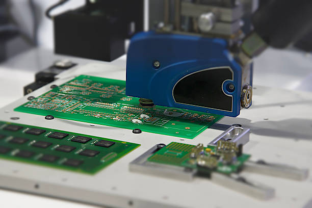
Why Choose Us as Your RF & Microwave PCB Manufacturer?
Eliminate multiple vendors and signal integrity risks. We manage the entire RF lifecycle in-house: high-precision fabrication, authorized component sourcing, and <±40μm SMT assembly.
We maintain bonded inventory of premium Rogers (RO4000/3000), Taconic, and Isola materials for rapid turnaround.
Pure PTFE boards are expensive. We expertly press Rogers laminates on outer signal layers with standard High-Tg FR4 cores. Achieve premium RF performance while reducing BOM costs.
Built for extreme environments. We manufacture to IPC Class 3 standards under IATF 16949 and ISO 13485 certified quality systems. Full traceability guaranteed.
Why Engineers Switch to Us
“PCBLion’s engineering team suggested a hybrid Rogers/FR4 stack-up and caught a critical impedance mismatch in our antenna feedline during DFM. They saved us a costly re-spin and improved our signal range.”
— Senior RF Engineer, Telecom Infrastructure
Applications We Support
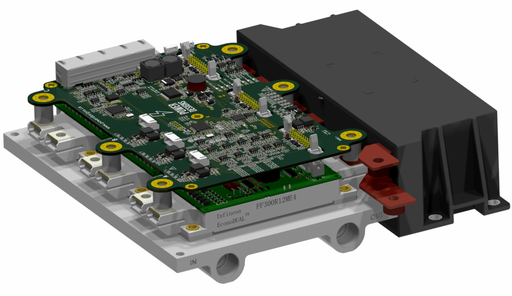
- Engine Control Units (ECU): 8-10 layer boards with -40°C to +125°C operating range
- ADAS Systems: 12-layer designs with controlled impedance for camera and radar modules
- Battery Management Systems (BMS): Heavy copper power planes (up to 18oz) combined with signal layers
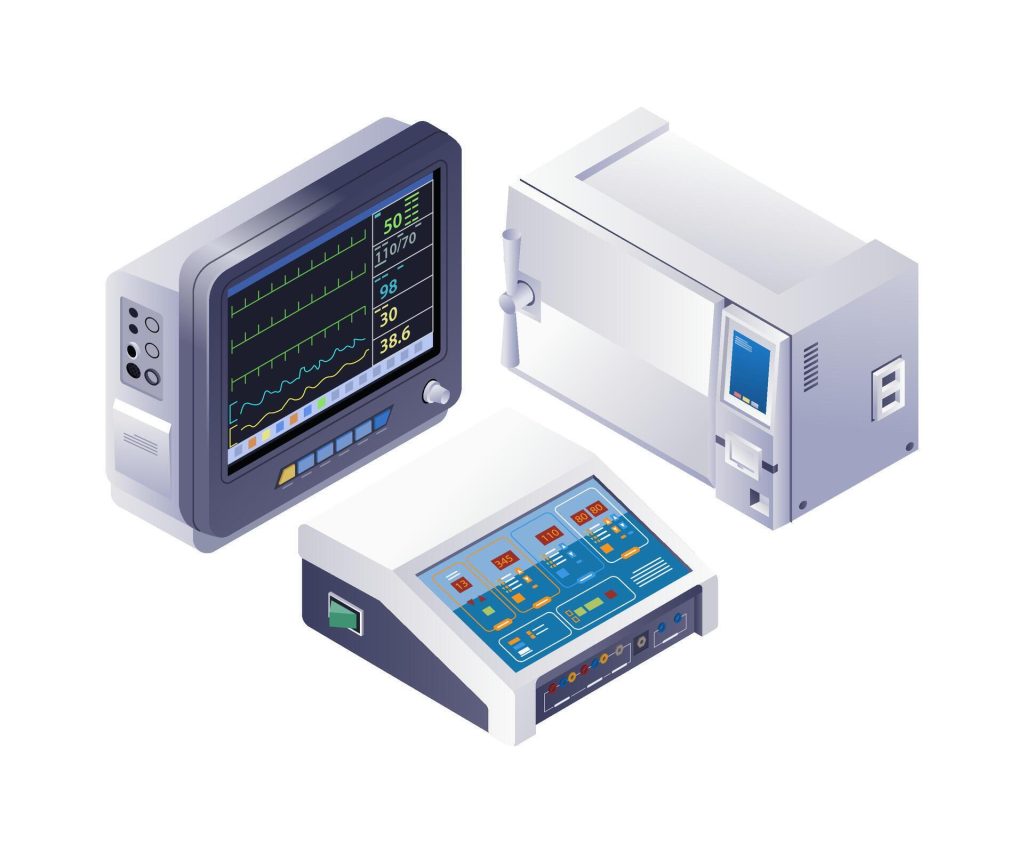
- Patient Monitoring: 6-8 layer boards with low-noise ground planes
- Diagnostic Equipment: 10-14 layer designs for high-speed data acquisition
- Implantable Devices: Rigid-flex multilayer integration for miniaturization
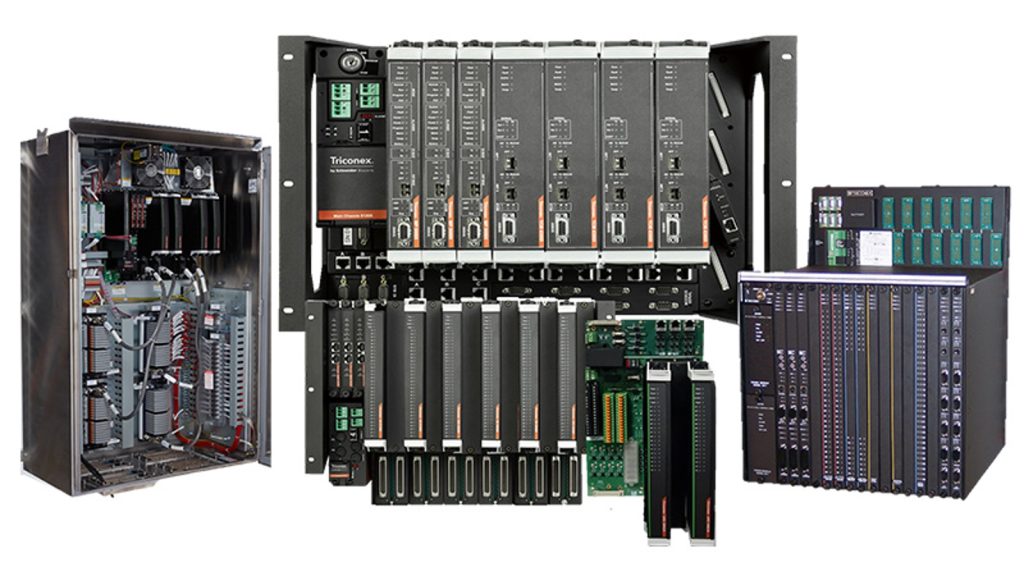
- PLC Controllers: 6-8 layer boards with robust EMI shielding
- Motor Drives: 8-10 layer power boards with 3-6oz copper
- Instrumentation: 10-12 layer precision analog designs with separate analog/digital ground planes
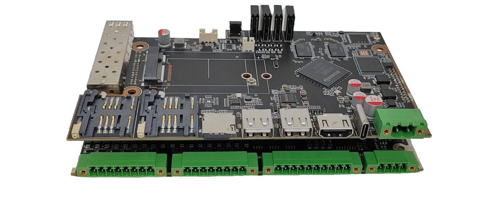
- 5G Base Stations: 12-16 layer RF boards with Rogers 4350B + FR4 hybrid stack-ups
- Gateway Devices: 6-8 layer designs balancing cost and performance
- Smart Sensors: 4-6 layer compact designs with integrated antennas
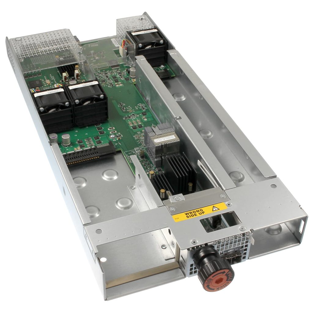
- Avionics: 20-40 layer high-reliability boards with ceramic substrates
- Satellite Communication: 12-20 layer boards with polyimide materials
- Navigation Systems: 10-16 layer precision designs with tight impedance control
Frequently Asked Questions
Do you stock high-frequency materials to support quick-turn prototypes?
Yes. We maintain a bonded inventory of premium high-frequency laminates, including Rogers, Taconic, and Isola. This allows us to start production immediately and deliver RF prototypes in as fast as 5-7 working days.
How do you ensure via reliability and signal integrity for PTFE-based microwave boards?
PTFE (Teflon) materials are inherently non-stick and notoriously difficult to plate. We utilize a rigorous Plasma Desmear process before plating to alter the hole-wall chemistry, ensuring robust copper adhesion and eliminating via failures during thermal cycling. Furthermore, we maintain ultra-tight trace etching tolerances down to ±0.0005″ (12.7µm) to mitigate “skin effect” losses and maintain strict ±5% impedance.
Can I combine standard FR4 with high-frequency materials to save cost?
Yes, this is a highly recommended practice known as a Hybrid Stack-up. We frequently laminate expensive RF materials (like Rogers or Taconic) on the critical outer signal layers, while using standard High-Tg FR4 for internal power and ground routing. This maintains excellent signal integrity while significantly reducing your overall board cost.
Start Your Project with a Trusted RF & Microwave PCB Manufacturer
Whether it’s a 4-layer prototype or a 40-layer production run, our engineering team is ready to provide free DFM feedback within hours.