
HDI PCB Fabrication
As a trusted HDI PCB Manufacturer, we know that when your design requires 0.35mm pitch BGAs, 01005 components, or 14+ layers in a compact form factor, traditional PCB technology hits a wall. HDI boards solve this by using laser-drilled microvias instead of mechanical drilling, enabling trace routing between layers that would be impossible otherwise.
Capabilities of OurHDI PCB ManufacturerFacility
| Capability Item | Specification / Details |
|---|---|
| Layer Count | 4 - 40 Layers (Mass Production) |
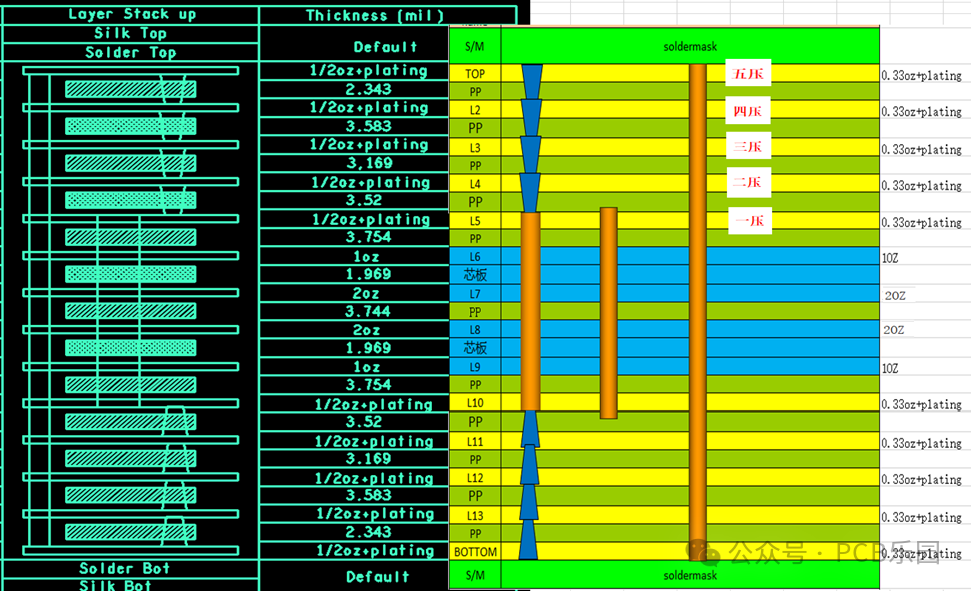
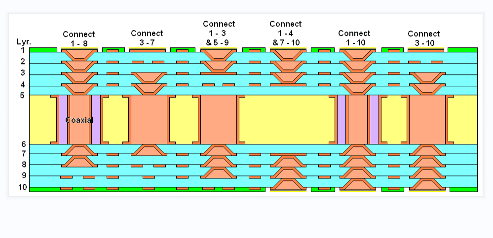
| HDI Structure | 1+N+1 to 7+N+7; Supports Any-Layer ELIC |
| Min. Trace / Space | 2mil / 2mil (0.05mm) - For fine pitch BGA fan-out |
| Min. Laser Drill | 0.075mm (3mil) [Requires 5mil Pad] |
| Min. Mech Drill | 0.15mm (6mil) |
| BGA Capabilities | Pitch: Down to 0.35mm |
| Via Technology | Blind, Buried, Stacked, Staggered, Skip Via, VIPPO |
| Board Thickness | 0.4mm - 8.0mm (Tolerance: ±10%) |
| Impedance Control | Single 50Ω / Diff 90Ω & 100Ω (±5% Tolerance) |
| Material Options | High-Tg FR4 (Tg170/180), Halogen-Free, Rogers/PTFE Hybrid |
| Copper Weight | Inner/Outer: 1/3oz - 3oz (Max) |
| Drill to Copper Space | 4mil (4-6L) / 5mil (8-12L) / 6mil (14L+) |
| Surface Finish | ENIG, ENEPIG, Immersion Silver, OSP, Hard Gold |
HDI PCB vs. Microvia PCB: Understanding the Distinction
This refers simply to a board that utilizes microvias (laser-drilled holes typically ≤ 0.15mm / 6mil) to connect adjacent layers. It is a specific feature.
HDI is the comprehensive architecture. It relies on microvias, but also mandates ultra-fine lines/spaces (often ≤ 3mil/3mil), advanced materials, and complex sequential lamination. All HDI boards use microvias, but not every board with a microvia qualifies as a true High-Density Interconnect system.
Advantages of HDI PCBs
HDI is the only reliable way to route high-I/O, ultra-fine pitch components without ballooning the board footprint.
Shorter trace lengths, closer ground planes, and the elimination of through-hole via stubs drastically reduce signal loss, cross-talk, and EMI/RFI issues in high-speed digital and RF applications
Copper-filled stacked microvias act as direct thermal conduits, pulling heat away from high-power components much faster than traditional mechanical vias.
While the bare HDI PCB costs more, it often allows engineers to combine multiple standard PCBs into one, reducing connectors, cables, assembly time, and final enclosure size.
Why leading OEMs accept the higher initial cost.
Transitioning to HDI isn’t just about shrinking the board; it’s a strategic engineering decision that impacts the entire product lifecycle
Critical HDI Design Rules We Verify
- Microvia Aspect Ratio: Maximum 1:1 (depth:diameter) for reliable plating
- Via-in-Pad Clearance: Minimum 0.15mm annular ring for non-filled vias
- Stacked Via Alignment: Maximum 0.05mm offset between stacks
- Trace-to-Microvia Spacing: Minimum 0.1mm to prevent acid trapping
- BGA Fan-out Strategy: Optimized routing for 0.35mm, 0.4mm, and 0.5mm pitch devices
- Layer-to-Copper Spacing: 4mil (4-6L), 5mil (8-12L), 6mil (14-18L)
- Minimum Pad Sizes: 5mil (3mil drill), 6mil (4mil drill), 8mil (6mil drill)
Quality Assurance for HDI Boards
In-Process Controls
- LDI Registration: ±25μm layer-to-layer alignment verified by optical measurement
- Microvia Inspection: 100% AOI (Automated Optical Inspection) after laser drilling
- Cross-Section Analysis: Random sampling (1 panel per 50) to verify via fill quality and copper plating thickness
Final Testing
- Electrical Test: Flying probe or fixture-based testing (100% net coverage)
- Impedance Test: Polar CITS500s with coupon verification (±5% tolerance achievable)
- Microsection: Provided upon request for first-article inspection (FAI)
Yield Performance
- PCB Fabrication Yield: >99.2% (tracked monthly, data available upon request)
- First Pass Yield (FPY): >99.0% for HDI boards with <10 layers
HDI Applications We Support
- Engine Control Units (ECU): 8-10 layer boards with -40°C to +125°C operating range
- ADAS Systems: 12-layer designs with controlled impedance for camera and radar modules
- Battery Management Systems (BMS): Heavy copper power planes (up to 18oz) combined with signal layers
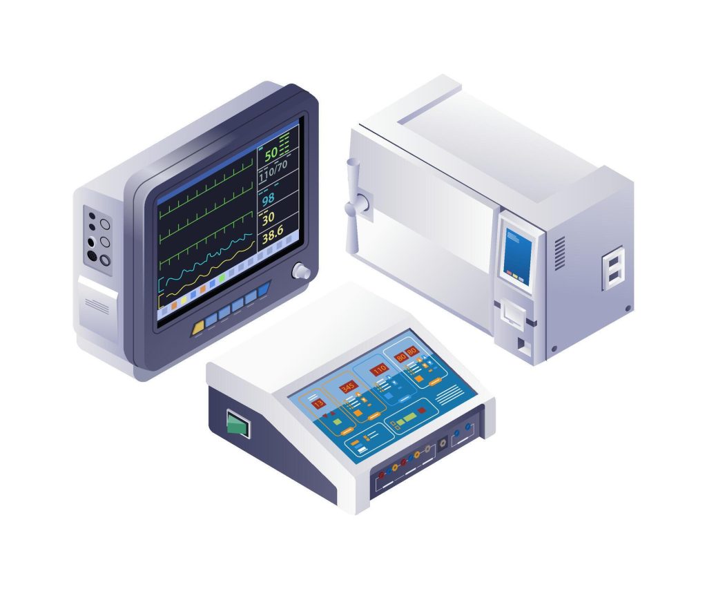
- Patient Monitoring: 6-8 layer boards with low-noise ground planes
- Diagnostic Equipment: 10-14 layer designs for high-speed data acquisition
- Implantable Devices: Rigid-flex multilayer integration for miniaturization
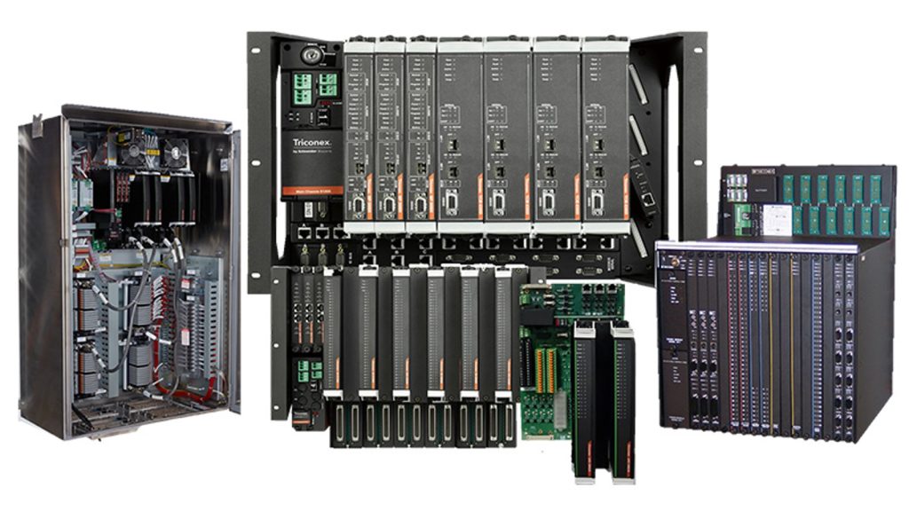
- PLC Controllers: 6-8 layer boards with robust EMI shielding
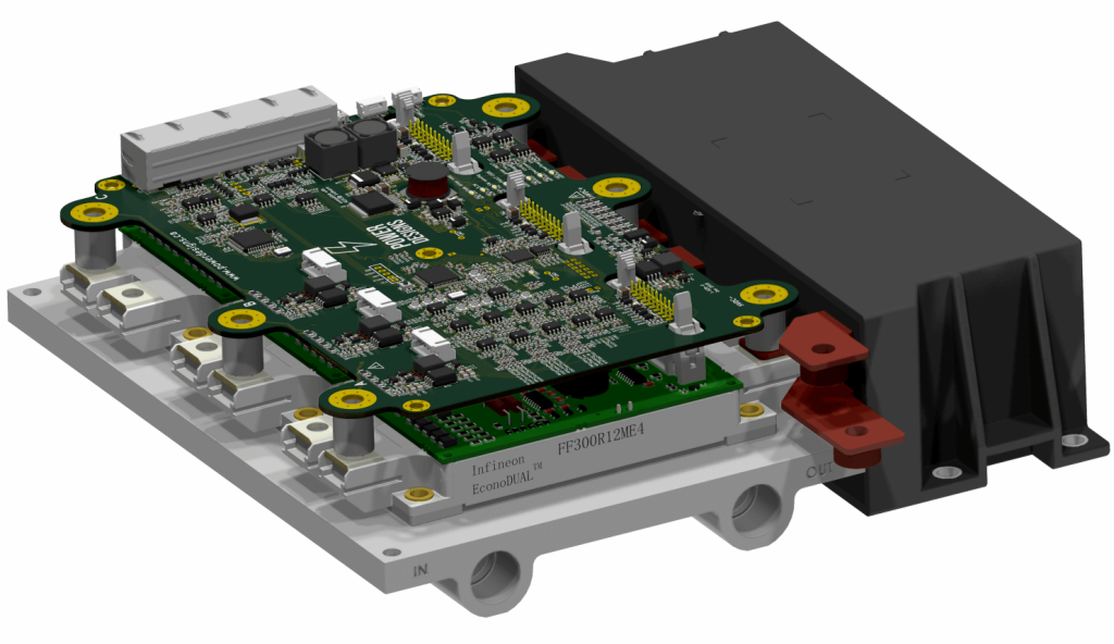
- Motor Drives: 8-10 layer power boards with 3-6oz copper
- Instrumentation: 10-12 layer precision analog designs with separate analog/digital ground planes
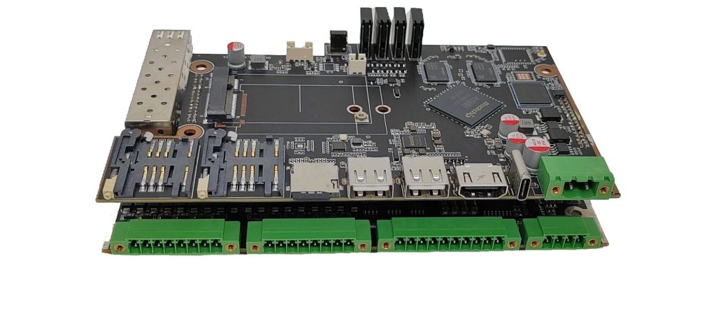
- 5G Base Stations: 12-16 layer RF boards with Rogers 4350B + FR4 hybrid stack-ups
- Gateway Devices: 6-8 layer designs balancing cost and performance
- Smart Sensors: 4-6 layer compact designs with integrated antennas
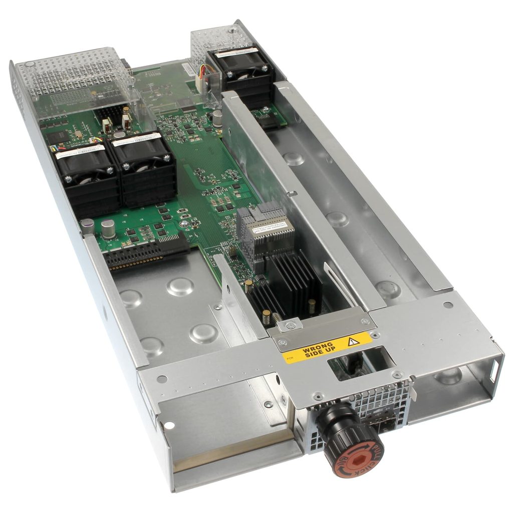
- Avionics: 20-40 layer high-reliability boards with ceramic substrates
- Satellite Communication: 12-20 layer boards with polyimide materials
- Navigation Systems: 10-16 layer precision designs with tight impedance control
Frequently Asked Questions
Can you produce multi-layer HDI boards with complex structures?
Yes, we manufacture HDI PCBs from 4 to 40 layers. Our advanced capabilities include 1+N+1 to 7+N+7 build-ups, as well as Any-Layer ELIC (Every Layer Interconnect) structures to meet the most demanding high-density routing requirements.
What is the typical lead time for manufacturing HDI PCBs?
Production time depends on the layer count and board complexity. Quick-turn prototypes (1-10 pcs) can be delivered in 5 to 7 working days, while standard mass production typically takes 10 to 15 working days.
How do you ensure the reliability and quality of your HDI boards?
We ensure zero-defect quality through mandatory DFM reviews, 100% Automated Optical Inspection (AOI) after laser drilling, precise impedance control via Polar TDR testing, and strict compliance with IPC Class 3 standards for high-reliability applications.
Start Your Project with a TrustedHDI PCB Manufacturer
Whether it’s a 4-layer prototype or a 40-layer production run, our engineering team is ready to provide free DFM feedback within hours.