
Heavy Copper PCB & Power PCB Manufacturer
PCBLion specializes in thick copper PCB and power PCB manufacturing, delivering precision-engineered boards with thick copper layers for high-current, high-power applications. We offer multi-layer designs, strict quality control, and expert engineering support to optimize your layouts. With industry certifications and a proven track record, we ensure durable, high-performance thick copper and power PCB solutions.
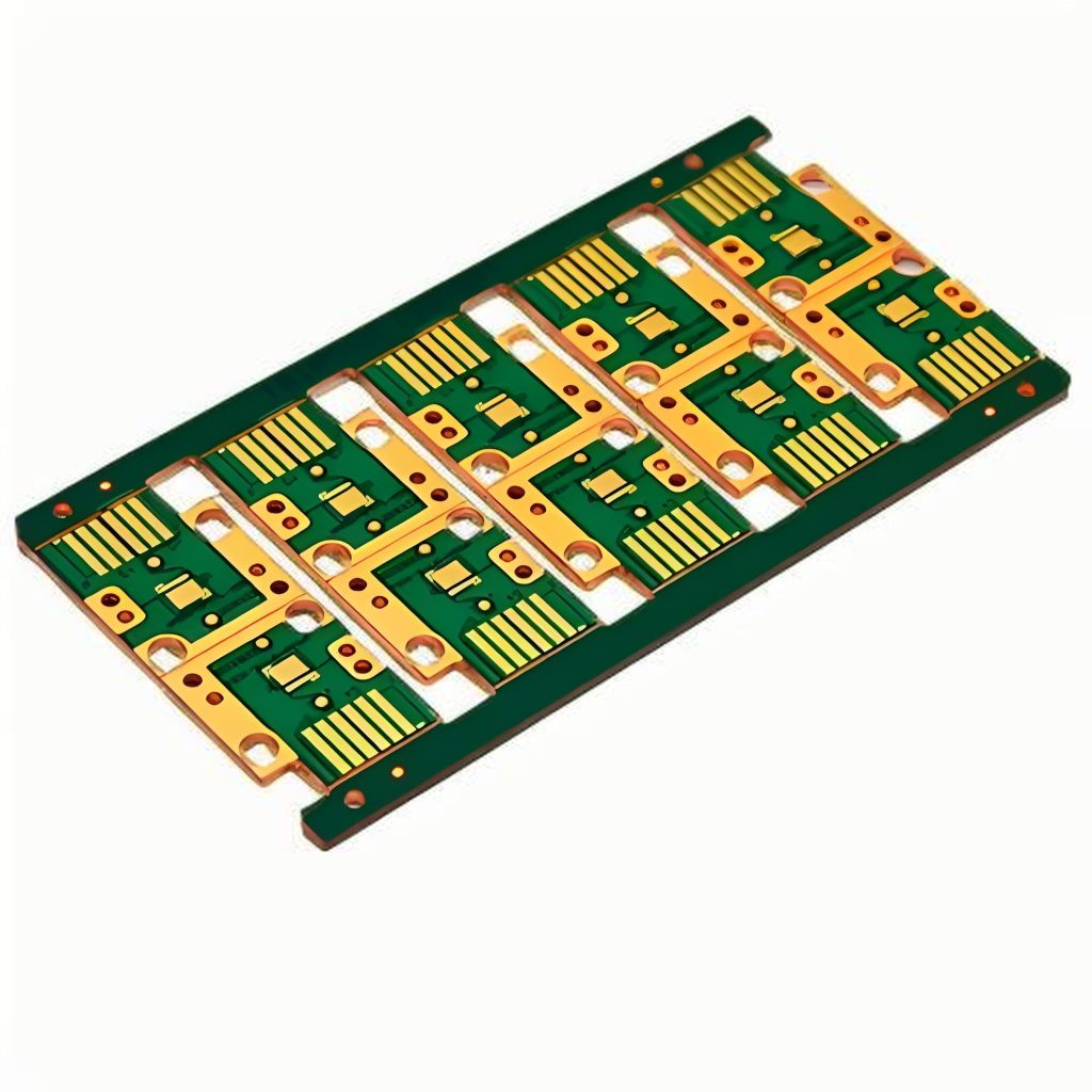
What Is Heavy Copper PCB?
When standard 1oz or 2oz traces cannot handle the thermal and electrical loads of your design, Heavy Copper PCBs (3oz to 20oz) are the definitive solution. By increasing the cross-sectional area of the copper without widening the traces, we empower your boards to handle extreme power densities.
Massive Current Carrying Capacity
Thicker copper layers easily handle continuous currents from 30A to over 500A without compromising performance. This eliminates the need for bulky, expensive external busbars and heavy wiring harnesses.
Advanced Thermal Management
Heavy copper significantly lowers the overall thermal resistance of the PCB. The board itself acts as a robust heat sink, rapidly dissipating heat away from critical high-power components like IGBTs and MOSFETs.
Compact Space Constraints
High power doesn't have to mean a large board. Heavy copper allows for high-current routing on fewer layers, enabling highly compact designs that reduce the overall dimensions and weight of your final product.
PCBLion's Heavy Copper PCB Manufacturing Capabilities
| Specification | Value |
|---|---|
| Layer Count | 1 to 8 layers |
| Max PCB Size | 500 x 1200mm |
| Metal Base Thickness | 0.8mm to 2.6mm |
| Finished Copper Thickness | 0.5oz to 4oz |
| Thermal Prepreg Thickness | 0.05mm to 0.2mm |
| Thermal Conductivity | 2.0 W/m·K to 6 W/m·K |
| Min Line Width / Space | 4mil / 4mil |
| Surface Finishes | HASL, ENIG, OSP, Immersion Tin |
| Dielectric Layer Material | Thermally conductive prepreg |
| Warpage | ≤0.75% |
| Electrical Strength | ≥3000V |
Heavy Copper & Power PCB Manufacturing Excellence
Beyond standard fabrication. PCBLion integrates advanced Etching Compensation and Thermal Stress Testing to deliver high-current PCBs that survive the most demanding environments.
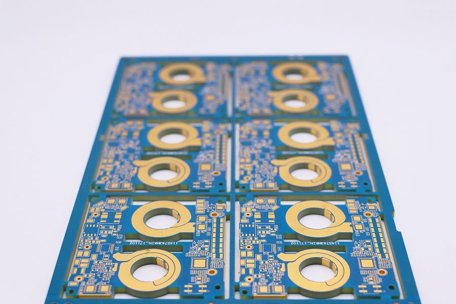
Overcoming the "Undercut" Challenge
In heavy copper fabrication, standard etching leads to severe undercut. PCBLion utilizes a Segmented Fast-Etch process combined with proprietary Etching Factor Compensation to ensure your final trace width meets electrical design requirements.
We use Multiple Screen Printing passes to ensure adequate coverage over high-profile copper traces, preventing "Skip-plating" and ensuring insulation reliability.
Every batch undergoes Micro-sectioning to verify dielectric thickness and Thermal Shock testing to ensure no delamination occurs during high-temp reflow.
Overcoming the Difficulties of Thick Copper Fabrication
Manufacturing PCBs with 4oz to 20oz copper is not simply about plating more metal. Extreme copper thickness introduces severe challenges such as chemical undercutting, dielectric voids, and drill wear. PCBLion utilizes proprietary engineering strategies—from specialized prepregs to advanced chemical controls—to ensure every heavy copper board meets strict IPC Class 3 reliability standards.
Prolonged chemical etching on thick copper causes severe side-etching (undercutting). We implement stepwise fast etching and dynamic compensation factors in the CAM stage to maintain perfectly rectangular trace profiles.
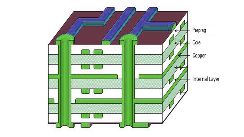
Thick copper creates deep "valleys" between traces. We use high-flow resins, silicone fillers, and materials with low CTE / high Td. Our extended high-temperature vacuum lamination prevents layer slippage and voids.
Drilling through 10oz copper generates massive heat and rough hole walls. We employ segmented drilling (step-drilling) and optimized feed/retract parameters to minimize drill wear and ensure smooth, reliable plated through-holes.
Why Choose PCBLion?
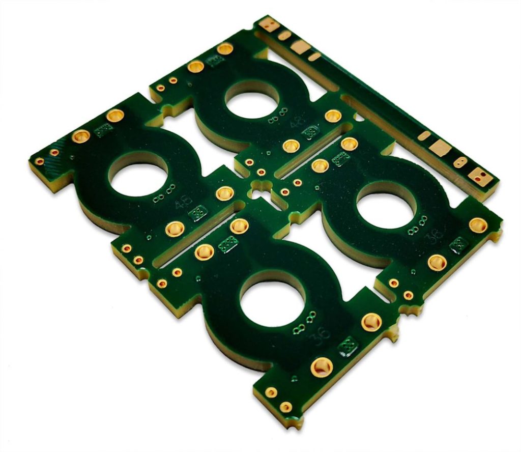
Up to 20oz outer layer and 12oz inner layer copper thickness. Precision-engineered for high-power distribution.
Utilization of High-Tg (170°C+) and Ceramic-filled laminates (Isola, Arlon) to mitigate CTE-related reliability risks.
Strict adherence to IPC-6012 Class 3 standards for Aerospace and Medical applications. Zero-defect philosophy.
Specialized Resin Filling and multi-stage vacuum lamination processes to eliminate internal micro-voids in thick copper layers.
Why Engineers Switch to Us
“PCBLion’s DFM review caught a Resin Filling issue on our 8-layer 6oz board that two other vendors missed. Their cross-section analysis proved they could maintain Hole Wall Copper integrity where others failed. They saved our project from a $15k scrap error.”
— Senior Power Electronics Engineer, EV Charging Systems
Applications We Support
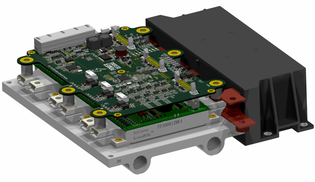
- Engine Control Units (ECU): 8-10 layer boards with -40°C to +125°C operating range
- ADAS Systems: 12-layer designs with controlled impedance for camera and radar modules
- Battery Management Systems (BMS): Heavy copper power planes (up to 18oz) combined with signal layers
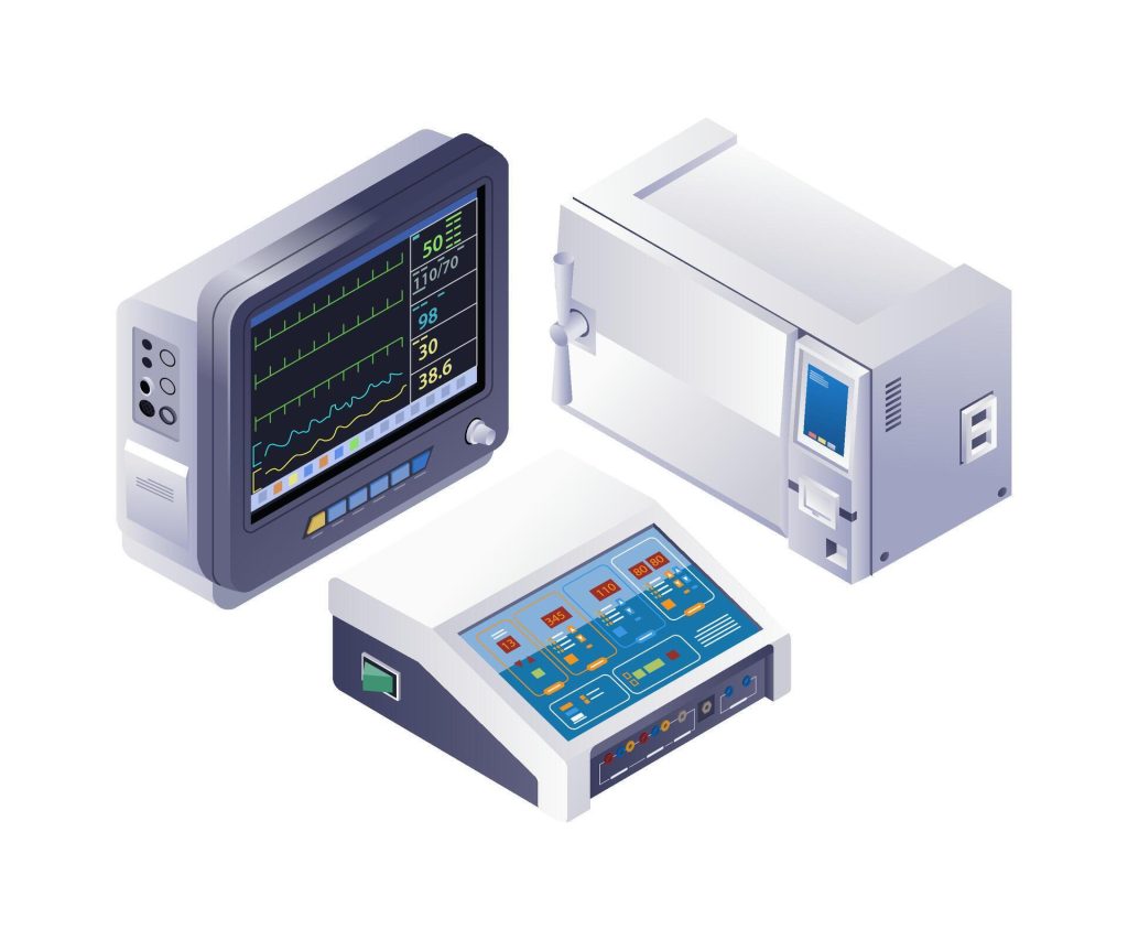
- Patient Monitoring: 6-8 layer boards with low-noise ground planes
- Diagnostic Equipment: 10-14 layer designs for high-speed data acquisition
- Implantable Devices: Rigid-flex multilayer integration for miniaturization
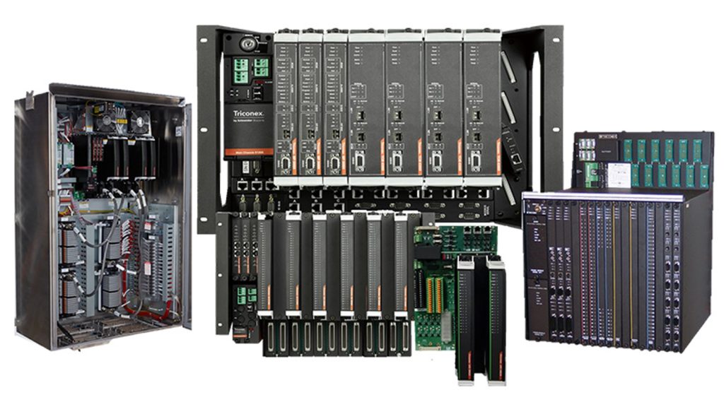
- PLC Controllers: 6-8 layer boards with robust EMI shielding
- Motor Drives: 8-10 layer power boards with 3-6oz copper
- Instrumentation: 10-12 layer precision analog designs with separate analog/digital ground planes
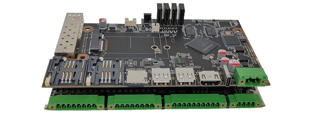
- 5G Base Stations: 12-16 layer RF boards with Rogers 4350B + FR4 hybrid stack-ups
- Gateway Devices: 6-8 layer designs balancing cost and performance
- Smart Sensors: 4-6 layer compact designs with integrated antennas
- Avionics: 20-40 layer high-reliability boards with ceramic substrates
- Satellite Communication: 12-20 layer boards with polyimide materials
- Navigation Systems: 10-16 layer precision designs with tight impedance control
Frequently Asked Questions
What kind of laminate is used to manufacture heavy copper PCBs?
Due to the high heat generated by heavy currents, standard FR4 is insufficient. We exclusively use High-Tg FR4 (Tg 170°C-180°C) or ceramic-based laminates. Materials from Shengyi, Kingboard, or Isola with a high Decomposition Temperature (Td) are selected to withstand elevated operating temperatures.
Can standard PCB lamination techniques be used with thick copper?
No. While we can safely sandwich up to 50 layers, heavy copper (e.g., 10 oz/ft²) requires careful process adjustments. We must use high-resin-content prepregs and customized vacuum press cycles to fill the deep gaps between thick copper traces without trapping air bubbles.
Heavy Copper vs. Aluminum vs. Ceramic PCB: Which should I choose?
Heavy Copper PCB: Best for managing massive currents and offering excellent 3D routing. Heaviest option.
Aluminum PCB: Highly cost-effective for general thermal dissipation (like LED lighting), but has a constrained current-carrying capacity compared to heavy copper.
Ceramic PCB: Offers the absolute best thermal conductivity for extreme heat/frequency, but is brittle, cannot handle massive currents like heavy copper, and comes at a premium cost.
Ready to Start Your Project?
Get an instant quote and see why thousands of engineers trust PCBLion for their PCB needs.